GUIDELINES FOR DESIGNING A PRINTED CIRCUIT BOARD
Designing a circuit board is both an art and science. So what’s needed to ensure a perfect design? I’ll lay it out here in five steps.
First, paying attention to PCB design is crucial for avoiding problems later. Creating a PCB is like conceiving the digital image and translating it into a physical entity. Thus, the circuit board design needs to be realistic enough to put on paper and convert into a tangible form.
1. Refine the component placement plan
While a PCB is not as vast as a landscape, you’re given a challenge to do wonders on a small piece of metal board. So, it’s important to ensure that the component placement plan is repeatedly revised to achieve the best use of the PCB. Hence:
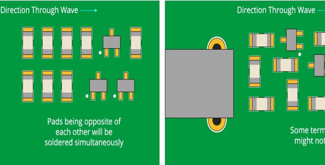
Pay attention to orientation: As a general rule, your PCB design should have similar components placed in a common orientation. This helps a lot during the soldering process, and errors are reduced.
